SFH617A
www.vishay.com
Vishay Semiconductors
Rev. 2.3, 14-Jan-13
1
Document Number: 83740
For technical questions, contact:
optocoupleranswers@vishay.com
THIS DOCUMENT IS SUBJECT TO CHANGE WITHOUT NOTICE. THE PRODUCTS DESCRIBED HEREIN AND THIS DOCUMENT
ARE SUBJECT TO SPECIFIC DISCLAIMERS, SET FORTH AT
www.vishay.com/doc?91000
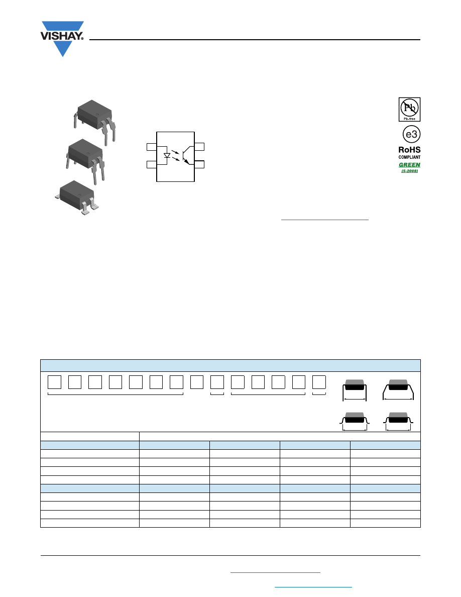
Optocoupler, Phototransistor Output, High Reliability,
5300 V
RMS
, 110 °C Rated
DESCRIPTION
The 110 °C rated SFH617A (DIP) feature a high current
transfer ratio, low coupling capacitance and high isolation
voltage. These couplers have a GaAs infrared diode emitter,
which is optically coupled to a silicon planar phototransistor
detector, and is incorporated in a plastic DIP-4 package.
The coupling devices are designed for signal transmission
between two electrically separated circuits.
The couplers are end-stackable with 2.54 mm spacing.
Creepage and clearance distances of > 8.0 mm are
achieved with option 6.
FEATURES
• Operating temperature from - 55 °C to + 110 °C
• Good CTR linearity depending on forward current
• Isolation test voltage, 5300 V
RMS
• High collector emitter voltage, V
CEO
= 70 V
• Low saturation voltage
• Fast switching times
• Low CTR degradation
• Temperature stable
• Low coupling capacitance
• End stackable, 0.100" (2.54 mm) spacing
• High common mode interference immunity
• Material categorization: For definitions of compliance
please see
www.vishay.com/doc?99912
APPLICATIONS
• AC adapter
• SMPS
• PLC
• Factory automation
• Game consoles
AGENCY APPROVALS
• UL1577, file no. E52744
• cUL tested to CSA 22.2 bulletin 5A
• DIN EN 60747-5-5 (VDE 0884-5) available with option 1
• BSI IEC 60950; IEC 60065
• FIMKO
• CQC
Notes
• Additional options may be possible, please contact sales office.
(1)
Also available in tubes; do not add T to end.
1
2
4
3
E
C
A
C
17918-20
ORDERING INFORMATION
S
F
H
6
1
7
A
-
#
X
0
#
#
T
PART NUMBER
CTR
BIN
PACKAGE OPTION
TAPE
AND
REEL
AGENCY CERTIFIED/PACKAGE
CTR (%)
UL, BSI, FIMKO, cUL
40 to 80
63 to 125
100 to 200
160 to 320
DIP-4
SFH617A-1
SFH617A-2
SFH617A-3
SFH617A-4
DIP-4, 400 mil, option 6
SFH617A-1X006
SFH617A-2X006
SFH617A-3X006
SFH617A-4X006
SMD-4, option 7
SFH617A-1X007T
-
SFH617A-3X007T
-
SMD-4, option 9
-
SFH617A-2X009T
-
-
VDE, UL, BSI, FIMKO, cUL
40 to 80
63 to 125
100 to 200
160 to 320
DIP-4
SFH617A-1X001
SFH617A-2X001
SFH617A-3X001
SFH617A-4X001
DIP-4, 400 mil, option 6
SFH617A-1X016
SFH617A-2X016
SFH617A-3X016
SFH617A-4X016
SMD-4, option 7
-
SFH617A-2X017T
SFH617A-3X017T
(1)
-
SMD-4, option 9
-
SFH617A-2X019T
(1)
-
-
7.62 mm
10.16 mm
Option 7
Option 6
Option 9
DIP-4
> 8 mm
8 mm typ.
SFH617A
www.vishay.com
Vishay Semiconductors
Rev. 2.3, 14-Jan-13
2
Document Number: 83740
For technical questions, contact:
optocoupleranswers@vishay.com
THIS DOCUMENT IS SUBJECT TO CHANGE WITHOUT NOTICE. THE PRODUCTS DESCRIBED HEREIN AND THIS DOCUMENT
ARE SUBJECT TO SPECIFIC DISCLAIMERS, SET FORTH AT
www.vishay.com/doc?91000
Notes
• Stresses in excess of the absolute maximum ratings can cause permanent damage to the device. Functional operation of the device is not
implied at these or any other conditions in excess of those given in the operational sections of this document. Exposure to absolute
maximum ratings for extended periods of the time can adversely affect reliability.
(1)
Refer to reflow profile for soldering conditions for surface mounted devices (SMD). Refer to wave profile for soldering conditions for through
hole devices (DIP).
Note
• Minimum and maximum values are testing requirements. Typical values are characteristics of the device and are the result of engineering
evaluation. Typical values are for information only and are not part of the testing requirements.
ABSOLUTE MAXIMUM RATINGS (T
amb
= 25 °C, unless otherwise specified)
PARAMETER
TEST CONDITION
SYMBOL
VALUE
UNIT
INPUT
Reverse voltage
V
R
6
V
Forward current
I
F
60
mA
Forward surge current
t
p
10 μs
I
FSM
2.5
A
LED power dissipation
at 25 °C
P
diss
70
mW
OUTPUT
Collector emitter voltage
V
CEO
70
V
Emitter collector voltage
V
ECO
7
V
Collector current
I
C
50
mA
Collector peak current
t
p
/T = 0.5, t
p
10 ms
I
CM
100
mA
Ouput power dissipation
at 25 °C
P
diss
150
mW
COUPLER
Isolation test voltage (RMS)
t = 1 min
V
ISO
5300
V
RMS
Isolation resistance
V
IO
= 500 V, T
amb
= 25 °C
R
IO
10
12
V
IO
= 500 V, T
amb
= 100 °C
R
IO
10
11
Operation temperature
T
amb
- 55 to + 110
°C
Storage temperature range
T
stg
- 55 to + 150
°C
Soldering temperature
(1)
2 mm from case,
10 s
T
sld
260
°C
ELECTRICAL CHARACTERISTICS (T
amb
= 25 °C, unless otherwise specified)
PARAMETER
TEST CONDITION
PART
SYMBOL
MIN.
TYP.
MAX.
UNIT
INPUT
Forward voltage
I
F
= 60 mA
V
F
1.35
1.65
V
Reverse current
V
R
= 6 V
I
R
0.01
10
μA
Capacitance
V
R
= 0 V, f = 1 MHz
C
O
13
pF
OUTPUT
Collector emitter capacitance
V
CE
= 5 V, f = 1 MHz
C
CE
5.2
pF
Collector emitter leakage current
V
CE
= 10 V
SFH617A-1
I
CEO
2
50
nA
SFH617A-2
I
CEO
2
50
nA
SFH617A-3
I
CEO
5
100
nA
SFH617A-4
I
CEO
5
100
nA
COUPLER
Collector emitter saturation voltage
I
F
= 10 mA, f = 1 MHz
V
CEsat
0.25
0.4
V
Coupling capacitance
C
C
0.4
pF
SFH617A
www.vishay.com
Vishay Semiconductors
Rev. 2.3, 14-Jan-13
3
Document Number: 83740
For technical questions, contact:
optocoupleranswers@vishay.com
THIS DOCUMENT IS SUBJECT TO CHANGE WITHOUT NOTICE. THE PRODUCTS DESCRIBED HEREIN AND THIS DOCUMENT
ARE SUBJECT TO SPECIFIC DISCLAIMERS, SET FORTH AT
www.vishay.com/doc?91000
CURRENT TRANSFER RATIO (T
amb
= 25 °C, unless otherwise specified)
PARAMETER
TEST CONDITION
PART
SYMBOL
MIN.
TYP.
MAX.
UNIT
I
C
/I
F
I
F
= 10 mA, V
CE
= 5 V
SFH617A-1
CTR
40
80
%
SFH617A-2
CTR
63
125
%
SFH617A-3
CTR
100
200
%
SFH617A-4
CTR
160
320
%
I
F
= 1 mA, V
CE
= 5 V
SFH617A-1
CTR
13
30
%
SFH617A-2
CTR
22
45
%
SFH617A-3
CTR
34
70
%
SFH617A-4
CTR
56
90
%
SWITCHING CHARACTERISTICS (T
amb
= 25 °C, unless otherwise specified)
PARAMETER
TEST CONDITION
PART
SYMBOL
MIN.
TYP.
MAX.
UNIT
NON-SATURATED
Turn-on time
I
F
= 10 mA, V
CC
= 5 V, R
L
= 75
t
on
3
μs
Rise time
I
F
= 10 mA, V
CC
= 5 V, R
L
= 75
t
r
2
μs
Turn-off time
I
F
= 10 mA, V
CC
= 5 V, R
L
= 75
t
off
2.3
μs
Fall time
I
F
= 10 mA, V
CC
= 5 V, R
L
= 75
t
f
2
μs
Cut-off frequency
I
F
= 10 mA, V
CC
= 5 V
f
CO
100
kHz
SATURATED
Turn-on time
I
F
= 20 mA
SFH617A-1
t
on
3
μs
I
F
= 10 mA
SFH617A-2
t
on
4.2
μs
SFH617A-3
t
on
4.2
μs
I
F
= 5 mA
SFH617A-4
t
on
6
μs
Rise time
I
F
= 20 mA
SFH617A-1
t
r
2
μs
I
F
= 10 mA
SFH617A-2
t
r
3
μs
SFH617A-3
t
r
3
μs
I
F
= 5 mA
SFH617A-4
t
r
4.6
μs
Turn-off time
I
F
= 20 mA
SFH617A-1
t
off
18
μs
I
F
= 10 mA
SFH617A-2
t
off
23
μs
SFH617A-3
t
off
23
μs
I
F
= 5 mA
SFH617A-4
t
off
25
μs
Fall time
I
F
= 20 mA
SFH617A-1
t
f
11
μs
I
F
= 10 mA
SFH617A-2
t
f
14
μs
SFH617A-3
t
f
14
μs
I
F
= 5 mA
SFH617A-4
t
f
15
μs
SFH617A
www.vishay.com
Vishay Semiconductors
Rev. 2.3, 14-Jan-13
4
Document Number: 83740
For technical questions, contact:
optocoupleranswers@vishay.com
THIS DOCUMENT IS SUBJECT TO CHANGE WITHOUT NOTICE. THE PRODUCTS DESCRIBED HEREIN AND THIS DOCUMENT
ARE SUBJECT TO SPECIFIC DISCLAIMERS, SET FORTH AT
www.vishay.com/doc?91000
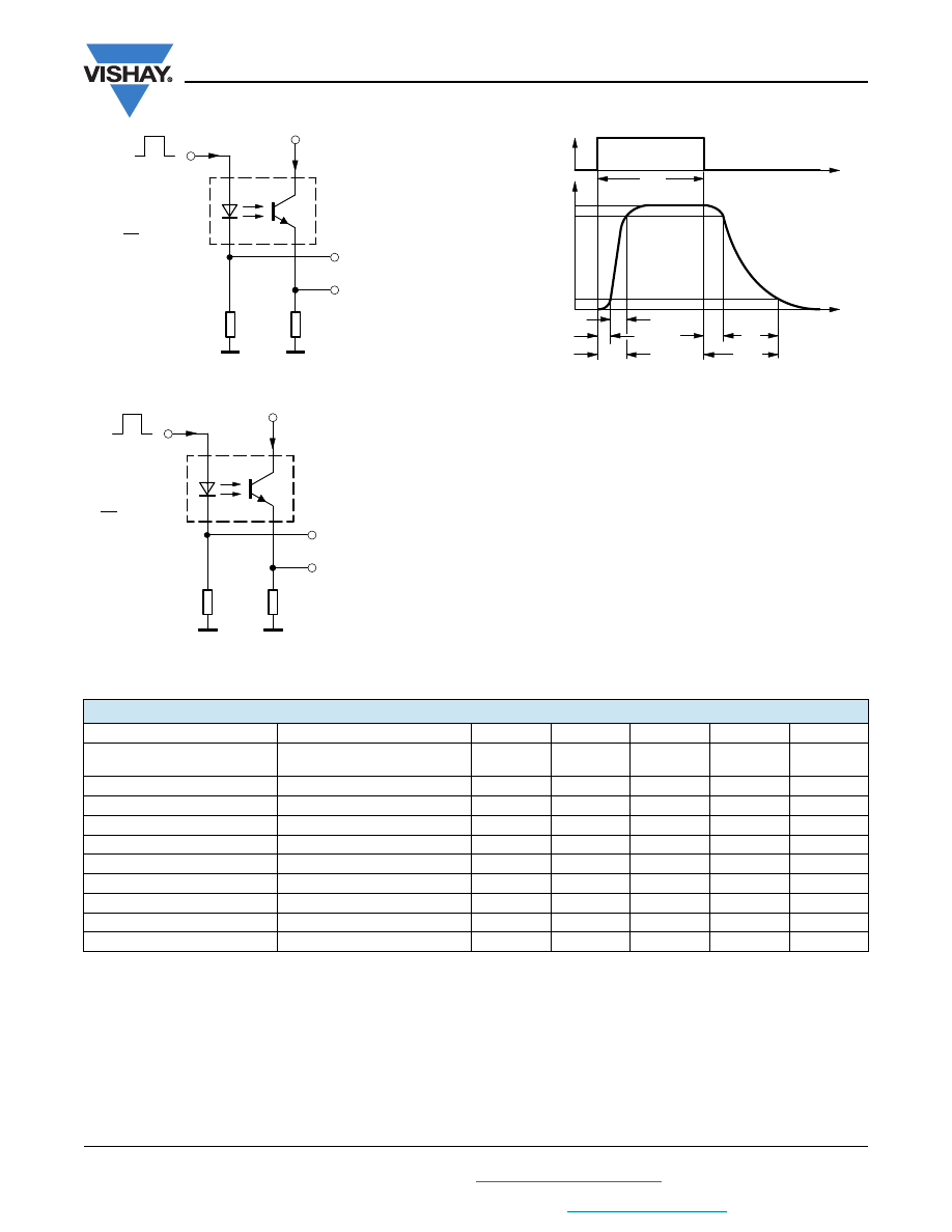
Fig. 1 - Test Circuit, Non-Saturated Operation
Fig. 2 - Test Circuit, Saturated Operation
Fig. 3 - Switching Times
Note
• According to DIN EN 60747-5-5 (VDE 0884-5). These optocouplers are suitable for “safe electrical insulation” only within the safety ratings.
Compliance with the safety ratings shall be ensured by means of protective circuits.
Channel I
Channel II
95 10804-3
R
G
= 50
Ω
t
p
t
p
= 50 µs
T
= 0.01
+ 5 V
I
F
0
50
Ω
R
L
I
F
Oscilloscope
R
L
= 1 M
Ω
C
L
= 20 pF
Channel I
Channel II
95 10843
R
G
= 50
Ω
t
p
t
p
= 50 µs
T
= 0.01
+ 5 V
I
C
I
F
0
50
Ω
1 k
Ω
I
F
= 10 mA
Oscilloscope
R
L
≥
C
L
20 pF
1 M
Ω
≤
t
p
t
t
0
0
10 %
90 %
100 %
t
r
t
d
t
on
t
s
t
f
t
off
I
F
I
C
t
p
Pulse duration
t
d
Delay time
t
r
Rise time
t
on
(= t
d
+ t
r
)
Turn-on time
t
s
Storage time
t
f
Fall time
t
off
(= t
s
+ t
f
)
Turn-off time
96 11698
SAFETY AND INSULATION RATINGS
PARAMETER
TEST CONDITION
SYMBOL
MIN.
TYP.
MAX.
UNIT
Climatic classification
(according to IEC 68 part 1)
55/110/21
Comparative tracking index
CTI
175
399
Rated impulse voltage
V
IOTM
8
kV
Maximum working voltages
Recurring peak voltage
V
IORM
890
V
Forward current
I
SI
275
mA
Power dissipation
P
SO
400
mW
Safety temperature
T
SI
175
°C
Creepage distance
7.0
mm
Clearance distance
7.0
mm
Isolation distance
per IEC 60950 2.10.5.1
0.4
mm
SFH617A
www.vishay.com
Vishay Semiconductors
Rev. 2.3, 14-Jan-13
5
Document Number: 83740
For technical questions, contact:
optocoupleranswers@vishay.com
THIS DOCUMENT IS SUBJECT TO CHANGE WITHOUT NOTICE. THE PRODUCTS DESCRIBED HEREIN AND THIS DOCUMENT
ARE SUBJECT TO SPECIFIC DISCLAIMERS, SET FORTH AT
www.vishay.com/doc?91000
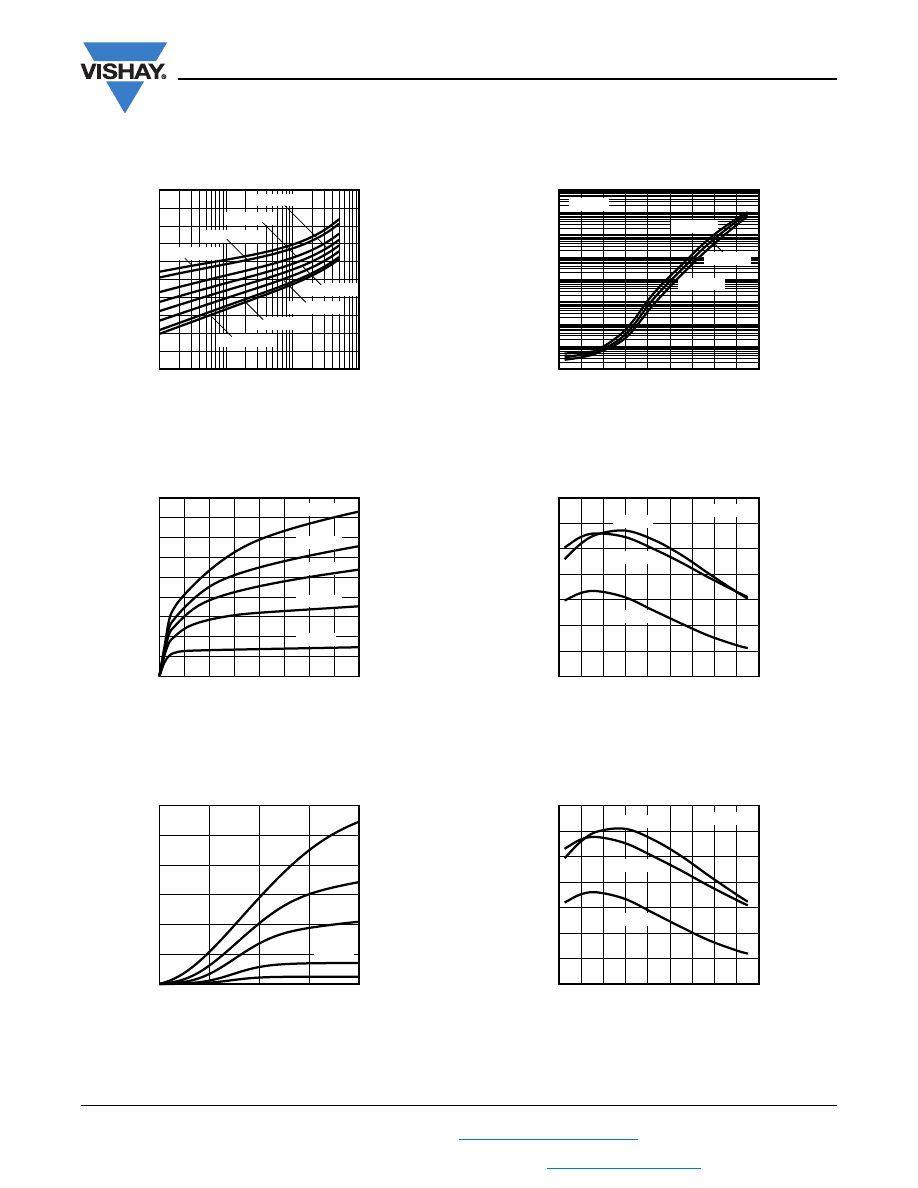
TYPICAL CHARACTERISTICS (T
amb
= 25 °C, unless otherwise specified)
Fig. 4 - Forward Voltage vs. Forward Current
Fig. 5 - Collector Current vs. Collector Emitter Voltage (NS)
Fig. 6 - Collector Current vs. Collector Emitter Voltage (sat)
Fig. 7 - Leakage Current vs. Ambient Temperature
Fig. 8 - Normalized CTR (NS) vs. Ambient Temperature
Fig. 9 - Normalized CTR (sat) vs. Ambient Temperature
0.6
0.8
0.9
1.0
1.1
1.2
1.3
1.4
1.6
0.1
1
10
100
I
F
- Forward Current (mA)
V
F
- Forward Voltage (V)
T
amb
= - 55 °C
1.5
0.7
T
amb
= - 40 °C
T
amb
= 0 °C
T
amb
= 25 °C
T
amb
= 50 °C
T
amb
= 75 °C
T
amb
= 100 °C
T
amb
= 110 °C
0
20
30
40
50
60
70
80
90
0
1
7
8
V
CE
- Collector Emitter Voltage (NS) (V)
I
C
- Collector Current (mA)
10
6
5
4
3
2
I
F
= 20 mA
I
F
= 15 mA
I
F
= 10 mA
I
F
= 30 mA
I
F
= 5 mA
0
10
15
20
30
0
0.4
V
CE
- Collector Emitter Voltage (sat) (V)
I
C
- Collector Current (mA)
5
0.3
0.2
0.1
25
I
F
= 10 mA
I
F
= 25 mA
I
F
= 5 mA
I
F
= 2 mA
I
F
= 1 mA
0.001
0.01
0.1
10
1
100
1000
100 000
- 60
120
T
amb
- Ambient Temperature (°C)
I
CE0
- Leakage Current (nA)
10 000
V
CE
= 40 V
- 40
100
80
60
40
20
0
- 20
I
F
= 0 mA
V
CE
= 12 V
V
CE
= 24 V
0
0.2
0.6
0.4
0.8
1.0
1.4
- 60
120
T
amb
- Ambient Temperature (°C)
CTR
Norm
- Normalized CTR (N
S
)
1.2
- 40
100
80
60
40
20
0
- 20
I
F
= 5 mA
I
F
= 10 mA
I
F
= 1 mA
V
CE
= 5 V
0
0.2
0.6
0.4
0.8
1.0
1.4
- 60
120
T
amb
- Ambient Temperature (°C)
CTR
Norm
- Normalized CTR (
s
at)
1.2
- 40
100
80
60
40
20
0
- 20
I
F
= 5 mA
I
F
= 10 mA
I
F
= 1 mA
V
CE
= 0.4 V
SFH617A
www.vishay.com
Vishay Semiconductors
Rev. 2.3, 14-Jan-13
6
Document Number: 83740
For technical questions, contact:
optocoupleranswers@vishay.com
THIS DOCUMENT IS SUBJECT TO CHANGE WITHOUT NOTICE. THE PRODUCTS DESCRIBED HEREIN AND THIS DOCUMENT
ARE SUBJECT TO SPECIFIC DISCLAIMERS, SET FORTH AT
www.vishay.com/doc?91000
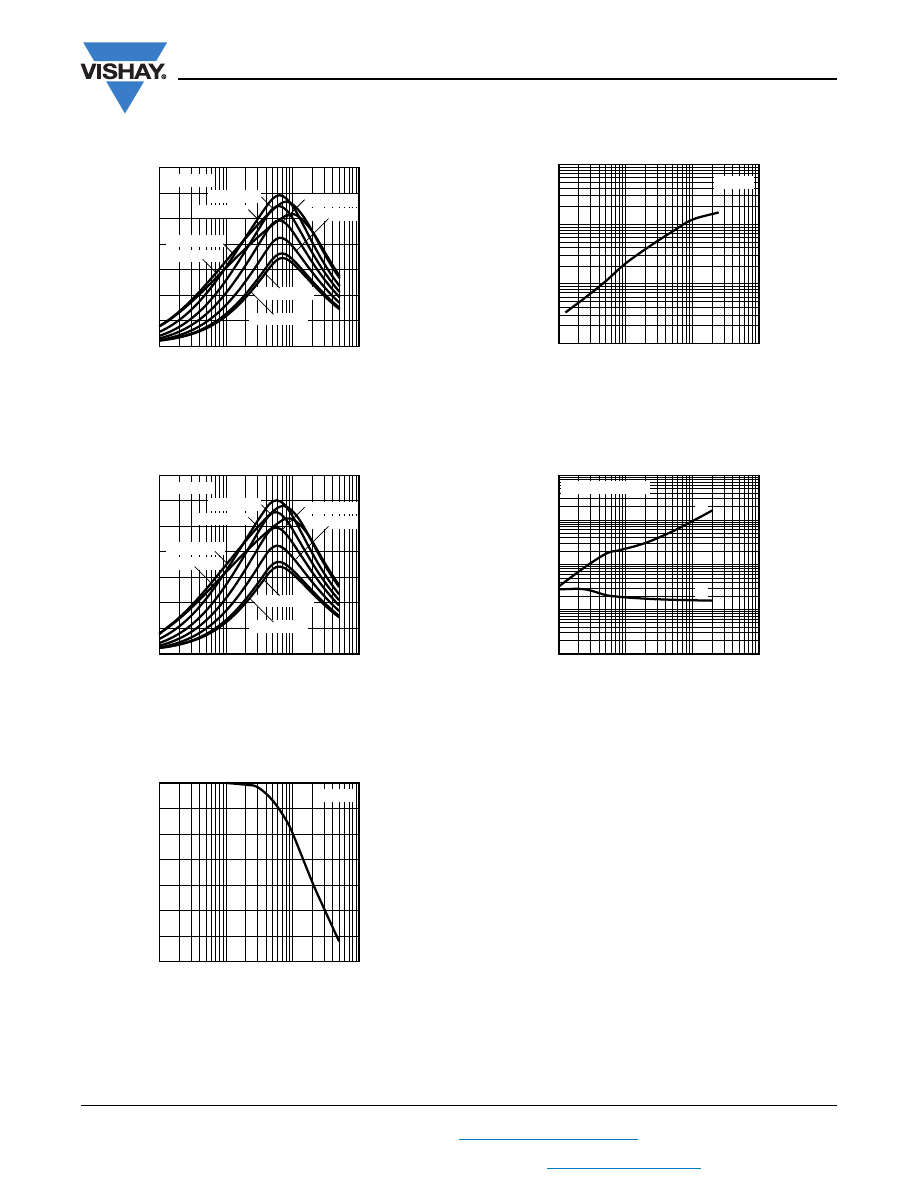
Fig. 10 - Normalized CTR (NS) vs. Forward Current
Fig. 11 - Normalized CTR (sat) vs. Forward Current
Fig. 12 - CTR Frequency vs. Phase Angle
Fig. 13 - CTR Frequency vs. Collector Current
Fig. 14 - Switching Time vs. Load Resistance
0
0.2
0.6
0.4
0.8
1.0
1.4
0.1
100
I
F
- Forward Current (mA)
CTR
Norm
- Normalized CTR (N
S
)
1.2
1
10
V
CE
= 10 V
T
amb
= - 55 °C
T
amb
= - 40 °C
T
amb
= 0 °C
T
amb
= 25 °C
T
amb
= 50 °C
T
amb
= 75 °C
T
amb
= 100 °C
T
amb
= 110 °C
0
0.2
0.6
0.4
0.8
1.0
1.4
0.1
100
I
F
- Forward Current (mA)
CTR
Norm
- Normalized CTR (
s
at)
1.2
1
10
T
amb
= - 55 °C
T
amb
= - 40 °C
T
amb
= 0 °C
T
amb
= 25 °C
T
amb
= 50 °C
T
amb
= 75 °C
T
amb
= 100 °C
T
amb
= 110 °C
V
CE
= 0.4 V
- 140
- 120
- 100
- 80
0
1
1000
f - Frequency (kHz)
Pha
s
e (deg)
- 20
10
100
V
CE
= 5 V
- 40
- 60
1
10
1000
0.1
100
I
C
- Collector Current (mA)
f
CTR
- CTR Fre
q
uency (kHz)
100
1
10
V
CC
= 5 V
0.1
1
10
1000
0.1
100
R
L
- Load Resistance (k
Ω)
t
on
, t
off
-
S
witching Time (μ
s
)
100
1
10
V
CE
= 5 V, I
F
= 10 mA
t
on
t
off
SFH617A
www.vishay.com
Vishay Semiconductors
Rev. 2.3, 14-Jan-13
7
Document Number: 83740
For technical questions, contact:
optocoupleranswers@vishay.com
THIS DOCUMENT IS SUBJECT TO CHANGE WITHOUT NOTICE. THE PRODUCTS DESCRIBED HEREIN AND THIS DOCUMENT
ARE SUBJECT TO SPECIFIC DISCLAIMERS, SET FORTH AT
www.vishay.com/doc?91000
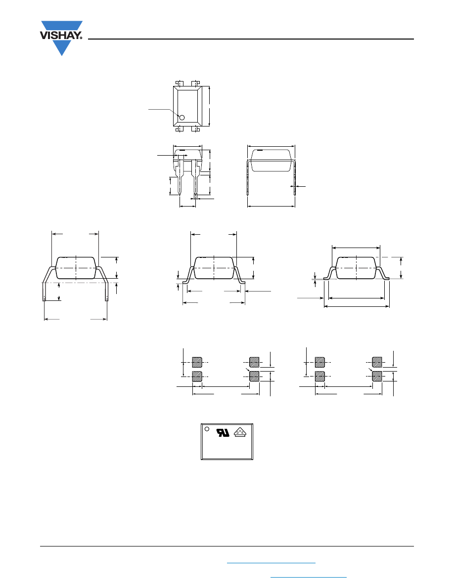
PACKAGE DIMENISONS in millimeters
PACKAGE MARKING
Notes
• VDE logo is only marked on option 1 parts. Option information is not marked on the part.
• Tape and reel suffix (T) is not part of the package marking.
i178027-10
6.5 ± 0.5
Pin 1 identifier
0.26
7.62 to 9.98
7.62 ± 0.3
4.58 ± 0.5
2.54 ± 0.25
0.5 ± 0.1
0.85 ± 0.1
2.8 ± 0.5
3.3 ± 0.5
3.5 ± 0.3
0.5 typ.
1
2
4
3
20802-28
2.54
1.78
0.76
8 min.
1.52
11.05
R 0.25
2.54
1.78
0.76
7.7
1.52
11.05
R 0.25
10.16 typ.
7.62 typ.
Option 6
3.5 ± 0.3
0.1 min.
2.7 min.
8 min.
7.62 typ.
3.5 ± 0.3
0.6 min.
10.16 ± 0.3
Option 7
0.35
+ 0.25
- 0.3
Option 9
7.62 typ.
0.6 min.
0.1 ± 0.1
3.5 ± 0.3
8.16 ± 0.8
10.16 ± 0.3
SFH617A-3
V YWW 25

Legal Disclaimer Notice
www.vishay.com
Vishay
Revision: 02-Oct-12
1
Document Number: 91000
Disclaimer
ALL PRODUCT, PRODUCT SPECIFICATIONS AND DATA ARE SUBJECT TO CHANGE WITHOUT NOTICE TO IMPROVE
RELIABILITY, FUNCTION OR DESIGN OR OTHERWISE.
Vishay Intertechnology, Inc., its affiliates, agents, and employees, and all persons acting on its or their behalf (collectively,
“Vishay”), disclaim any and all liability for any errors, inaccuracies or incompleteness contained in any datasheet or in any other
disclosure relating to any product.
Vishay makes no warranty, representation or guarantee regarding the suitability of the products for any particular purpose or
the continuing production of any product. To the maximum extent permitted by applicable law, Vishay disclaims (i) any and all
liability arising out of the application or use of any product, (ii) any and all liability, including without limitation special,
consequential or incidental damages, and (iii) any and all implied warranties, including warranties of fitness for particular
purpose, non-infringement and merchantability.
Statements regarding the suitability of products for certain types of applications are based on Vishay’s knowledge of typical
requirements that are often placed on Vishay products in generic applications. Such statements are not binding statements
about the suitability of products for a particular application. It is the customer’s responsibility to validate that a particular
product with the properties described in the product specification is suitable for use in a particular application. Parameters
provided in datasheets and/or specifications may vary in different applications and performance may vary over time. All
operating parameters, including typical parameters, must be validated for each customer application by the customer’s
technical experts. Product specifications do not expand or otherwise modify Vishay’s terms and conditions of purchase,
including but not limited to the warranty expressed therein.
Except as expressly indicated in writing, Vishay products are not designed for use in medical, life-saving, or life-sustaining
applications or for any other application in which the failure of the Vishay product could result in personal injury or death.
Customers using or selling Vishay products not expressly indicated for use in such applications do so at their own risk. Please
contact authorized Vishay personnel to obtain written terms and conditions regarding products designed for such applications.
No license, express or implied, by estoppel or otherwise, to any intellectual property rights is granted by this document or by
any conduct of Vishay. Product names and markings noted herein may be trademarks of their respective owners.
Material Category Policy
Vishay Intertechnology, Inc. hereby certifies that all its products that are identified as RoHS-Compliant fulfill the
definitions and restrictions defined under Directive 2011/65/EU of The European Parliament and of the Council
of June 8, 2011 on the restriction of the use of certain hazardous substances in electrical and electronic equipment
(EEE) - recast, unless otherwise specified as non-compliant.
Please note that some Vishay documentation may still make reference to RoHS Directive 2002/95/EC. We confirm that
all the products identified as being compliant to Directive 2002/95/EC conform to Directive 2011/65/EU.
Vishay Intertechnology, Inc. hereby certifies that all its products that are identified as Halogen-Free follow Halogen-Free
requirements as per JEDEC JS709A standards. Please note that some Vishay documentation may still make reference
to the IEC 61249-2-21 definition. We confirm that all the products identified as being compliant to IEC 61249-2-21
conform to JEDEC JS709A standards.
Wyszukiwarka
Podobne podstrony:
BYV27 50 BYV27 200 (Vishay)
BF970 Vishay elenota pl
BF966S (Vishay)
BZX79 x2V4 x75 (Vishay)
SFH628A, SFH6286 (Vishay)
Si3430DV (Vishay)
XT26T (Vishay)
SUP40N25 60 (Vishay)
Vishay LTO 50
SFH615A, SFH6156 (Vishay)
BPW96 (Vishay)
XT49M (Vishay)
SUB65P06 20, SUP65P06 20 (Vishay)
MOC8050 (Vishay)
TCZT8020 (Vishay)
SFH618x (Vishay)
XO 523 (Vishay)
TSOP17xx (Vishay)
więcej podobnych podstron