FEATURES
D High-Efficiency PWM Optimized
D 100% R
g
Tested
Si3430DV
Vishay Siliconix
Document Number: 71235
S-31725—Rev. B, 18-Aug-03
www.vishay.com
N-Channel 100-V (D-S) MOSFET
PRODUCT SUMMARY
V
DS
(V)
r
DS(on)
(W)
I
D
(A)
100
0.170 @ V
GS
= 10 V
2.4
100
0.185 @ V
GS
= 6.0 V
2.3
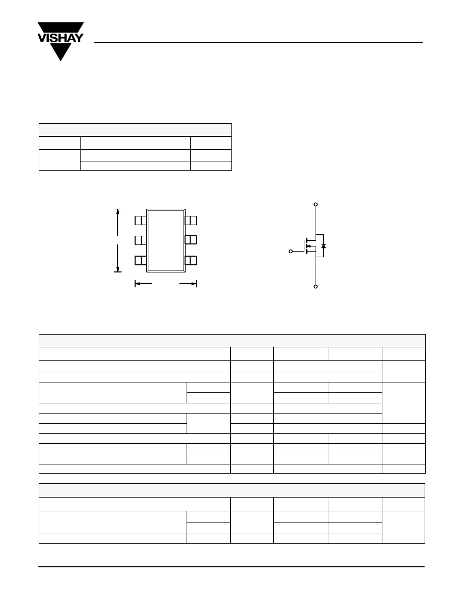
(1, 2, 5, 6) D
(3) G
(4) S
N-Channel MOSFET
TSOP-6
Top View
6
4
1
2
3
5
2.85 mm
3 mm
Ordering Information: Si3430DV-T1
ABSOLUTE MAXIMUM RATINGS (T
A
= 25_C UNLESS OTHERWISE NOTED)
Parameter
Symbol
5 secs
Steady State
Unit
Drain-Source Voltage
V
DS
100
V
Gate-Source Voltage
V
GS
"20
V
Continuous Drain Current
(T
J
= 175_C)
T
A
= 25_C
I
D
2.4
1.8
Continuous Drain Current
(T
J
= 175_C)
T
A
= 85_C
I
D
1.7
1.3
A
Pulsed Drain Current
I
DM
8
A
Avalanche Current
L = 0 1 mH
I
AR
6
Repetitive Avalanche Energy (Duty Cycle v1%)
L = 0.1 mH
E
AR
1.8
mJ
Continuous Source Current (Diode Conduction)
I
S
1.7
1.0
A
Maximum Power Dissipation
T
A
= 25_C
P
D
2.0
1.14
W
Maximum Power Dissipation
T
A
= 85_C
P
D
1.0
0.59
W
Operating Junction and Storage Temperature Range
T
J
, T
stg
-55 to 150
_C
THERMAL RESISTANCE RATINGS
Parameter
Symbol
Typical
Maximum
Unit
M i
J
ti
t A bi t
t v 5 sec
R
45
62.5
Steady State
R
thJA
90
110
_C/W
Maximum Junction-to-Foot (Drain)
Steady State
R
thJF
25
30
C/W
Notes
a.
Surface Mounted on 1” x 1” FR4 Board.
Si3430DV
Vishay Siliconix
www.vishay.com
Document Number: 71235
S-31725—Rev. B, 18-Aug-03
SPECIFICATIONS (T
J
= 25_C UNLESS OTHERWISE NOTED)
Parameter
Symbol
Test Condition
Min
Typ
Max
Unit
Static
Gate Threshold Voltage
V
GS(th)
V
DS
= V
GS
, I
D
= 250 mA
2
V
Gate-Body Leakage
I
GSS
V
DS
= 0 V, V
GS
= "20 V
"100
nA
Zero Gate Voltage Drain Current
I
DSS
V
DS
= 80 V, V
GS
= 0 V
1
mA
Zero Gate Voltage Drain Current
I
DSS
V
DS
= 80 V, V
GS
= 0 V, T
J
= 85_C
25
mA
I
D(on)
V
DS
w 5 V, V
GS
= 10
V
8
A
Drain-Source On-State Resistance
r
DS(on)
V
GS
= 10
V, I
D
= 2.4 A
0.148
0.170
W
Drain-Source On-State Resistance
r
DS(on)
V
GS
= 6.0 V, I
D
= 2.3 A
0.160
0.185
W
Forward Transconductance
g
fs
V
DS
= 15 V, I
D
= 2.4 A
7
S
Diode Forward Voltage
V
SD
I
S
= 1.7 A, V
GS
= 0 V
0.8
1.2
V
Dynamic
Total Gate Charge
Q
g
5.5
6.6
Gate-Source Charge
Q
gs
V
DS
= 50 V,
V
GS
= 10 V, I
D
= 2.4 A
1.5
nC
Gate-Drain Charge
Q
gd
1.4
Gate Resistance
R
g
1
4
W
Turn-On Delay Time
t
d(on)
9
20
Rise Time
t
r
V
DD
= 50 V, R
L
= 50 W
11
20
ns
Turn-Off Delay Time
t
d(off)
V
DD
= 50 V, R
L
= 50 W
I
D
^ 1 A, V
GEN
= 10 V, R
G
= 6 W
16
30
ns
Fall Time
t
f
9
20
Gate Resistance
R
g
V
GS
= 0.1 V, f = 5 MHz
2.8
W
Source-Drain Reverse Recovery Time
t
rr
I
F
= 1.7 A, di/dt = 100 A/ms
50
80
ns
Notes
a.
Pulse test; pulse width v
300 ms, duty cycle v
2%.
b.
Guaranteed by design, not subject to production testing.
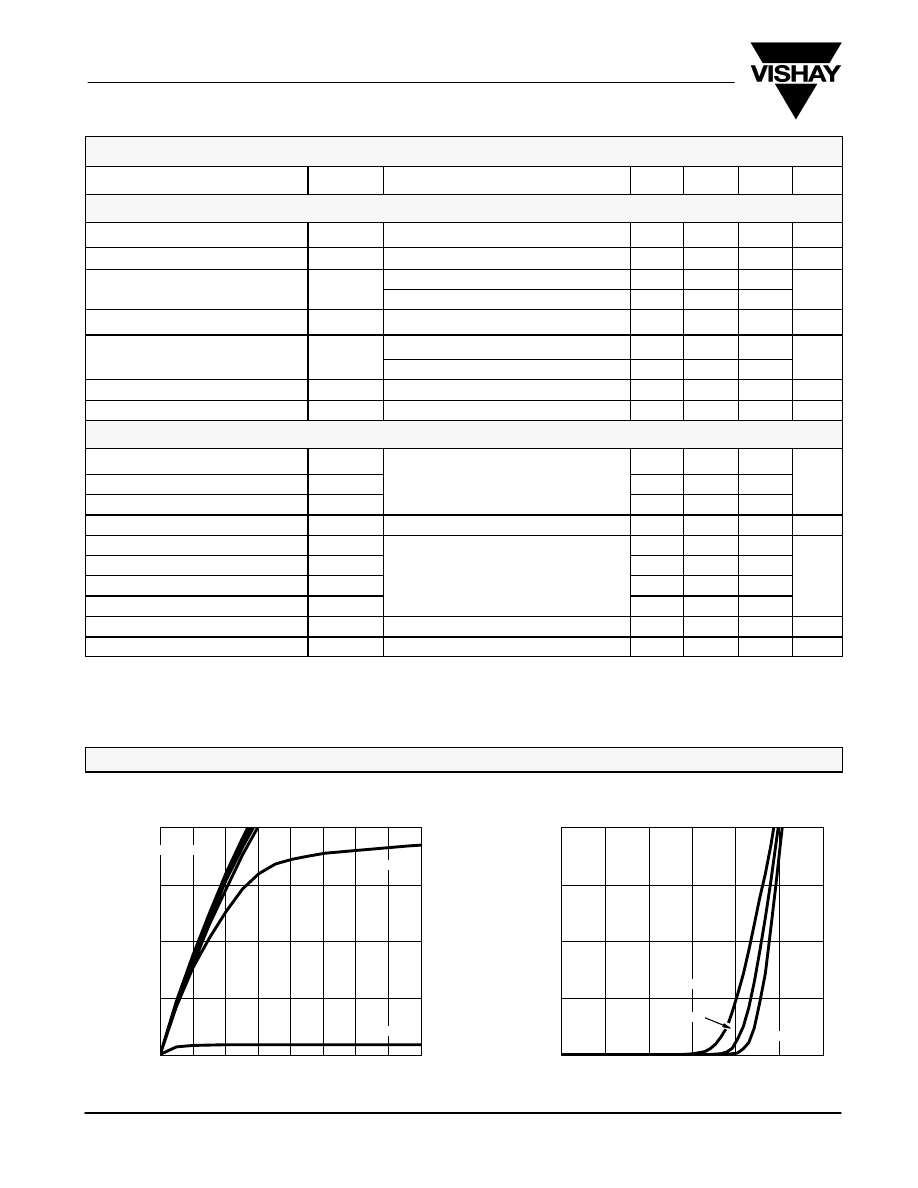
TYPICAL CHARACTERISTICS (25_C UNLESS NOTED)
0
2
4
6
8
0
1
2
3
4
5
6
0
2
4
6
8
0.0
0.5
1.0
1.5
2.0
2.5
3.0
3.5
4.0
V
GS
= 10 thru 6 V
T
C
= 125_C
-55_C
4 V
25_C
Output Characteristics
Transfer Characteristics
V
DS
- Drain-to-Source Voltage (V)
- Drain Current (A)
I
D
V
GS
- Gate-to-Source Voltage (V)
- Drain Current (A)
I
D
5 V
Si3430DV
Vishay Siliconix
Document Number: 71235
S-31725—Rev. B, 18-Aug-03
www.vishay.com
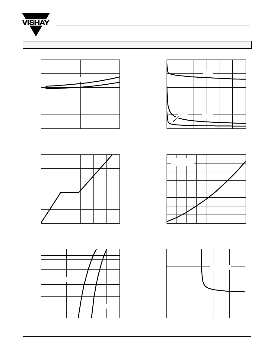
TYPICAL CHARACTERISTICS (25_C UNLESS NOTED)
- On-Resistance (
r
DS(on)
W
)
0
100
200
300
400
500
0
10
20
30
40
50
60
0.6
0.8
1.0
1.2
1.4
1.6
1.8
2.0
2.2
-50
-25
0
25
50
75
100
125
150
0
2
4
6
8
10
0
1
2
3
4
5
6
0.00
0.05
0.10
0.15
0.20
0.25
0
2
4
6
8
V
DS
- Drain-to-Source Voltage (V)
C
rss
C
oss
C
iss
V
DS
= 50 V
I
D
= 2.4 A
I
D
- Drain Current (A)
V
GS
= 10 V
I
D
= 2.4 A
V
GS
= 10 V
V
GS
= 6.0 V
Gate Charge
On-Resistance vs. Drain Current
- Gate-to-Source V
oltage (V)
Q
g
- Total Gate Charge (nC)
C
- Capacitance (pF)
V
GS
Capacitance
On-Resistance vs. Junction Temperature
T
J
- Junction Temperature (_C)
(Normalized)
- On-Resistance (
r
DS(on)
W
)
0.0
0.2
0.4
0.6
0.8
1.0
1.2
0.0
0.1
0.2
0.3
0.4
0
2
4
6
8
10
T
J
= 150_C
T
J
= 25_C
I
D
= 2.4 A
10
1
Source-Drain Diode Forward Voltage
On-Resistance vs. Gate-to-Source Voltage
- On-Resistance (
r
DS(on)
W
)
V
SD
- Source-to-Drain Voltage (V)
V
GS
- Gate-to-Source Voltage (V)
- Source Current (A)
I
S
Si3430DV
Vishay Siliconix
www.vishay.com
Document Number: 71235
S-31725—Rev. B, 18-Aug-03
TYPICAL CHARACTERISTICS (25_C UNLESS NOTED)
0
15
30
5
10
Power (W)
Single Pulse Power
Time (sec)
10
-3
10
-2
1
10
600
10
-1
10
-4
100
-1.0
-0.8
-0.6
-0.4
-0.2
-0.0
0.2
0.4
0.6
-50
-25
0
25
50
75
100
125
150
I
D
= 250 mA
2
1
0.1
0.01
0.2
0.1
0.05
0.02
Single Pulse
Duty Cycle = 0.5
Threshold Voltage
Variance (V)
V
GS(th)
T
J
- Temperature (_C)
Normalized Thermal Transient Impedance, Junction-to-Ambient
Square Wave Pulse Duration (sec)
Normalized Ef
fective
Transient
Thermal Impedance
1. Duty Cycle, D =
2. Per Unit Base = R
thJA
= 90_C/W
3. T
JM
- T
A
= P
DM
Z
thJA(t)
t
1
t
2
t
1
t
2
Notes:
4. Surface Mounted
P
DM
10
-3
10
-2
1
10
10
-1
10
-4
2
1
0.1
0.01
0.2
0.1
0.05
0.02
Single Pulse
Duty Cycle = 0.5
Normalized Thermal Transient Impedance, Junction-to-Foot
Square Wave Pulse Duration (sec)
Normalized Ef
fective
Transient
Thermal Impedance
1
600
10
20
0.1
0.01
100
25
Document Outline
- Datasheet
- Disclaimer
Wyszukiwarka
Podobne podstrony:
BYV27 50 BYV27 200 (Vishay)
BF970 Vishay elenota pl
BF966S (Vishay)
BZX79 x2V4 x75 (Vishay)
SFH628A, SFH6286 (Vishay)
XT26T (Vishay)
SUP40N25 60 (Vishay)
Vishay LTO 50
SFH615A, SFH6156 (Vishay)
BPW96 (Vishay)
XT49M (Vishay)
SFH617A [Vishay]
SUB65P06 20, SUP65P06 20 (Vishay)
MOC8050 (Vishay)
TCZT8020 (Vishay)
SFH618x (Vishay)
XO 523 (Vishay)
TSOP17xx (Vishay)
więcej podobnych podstron