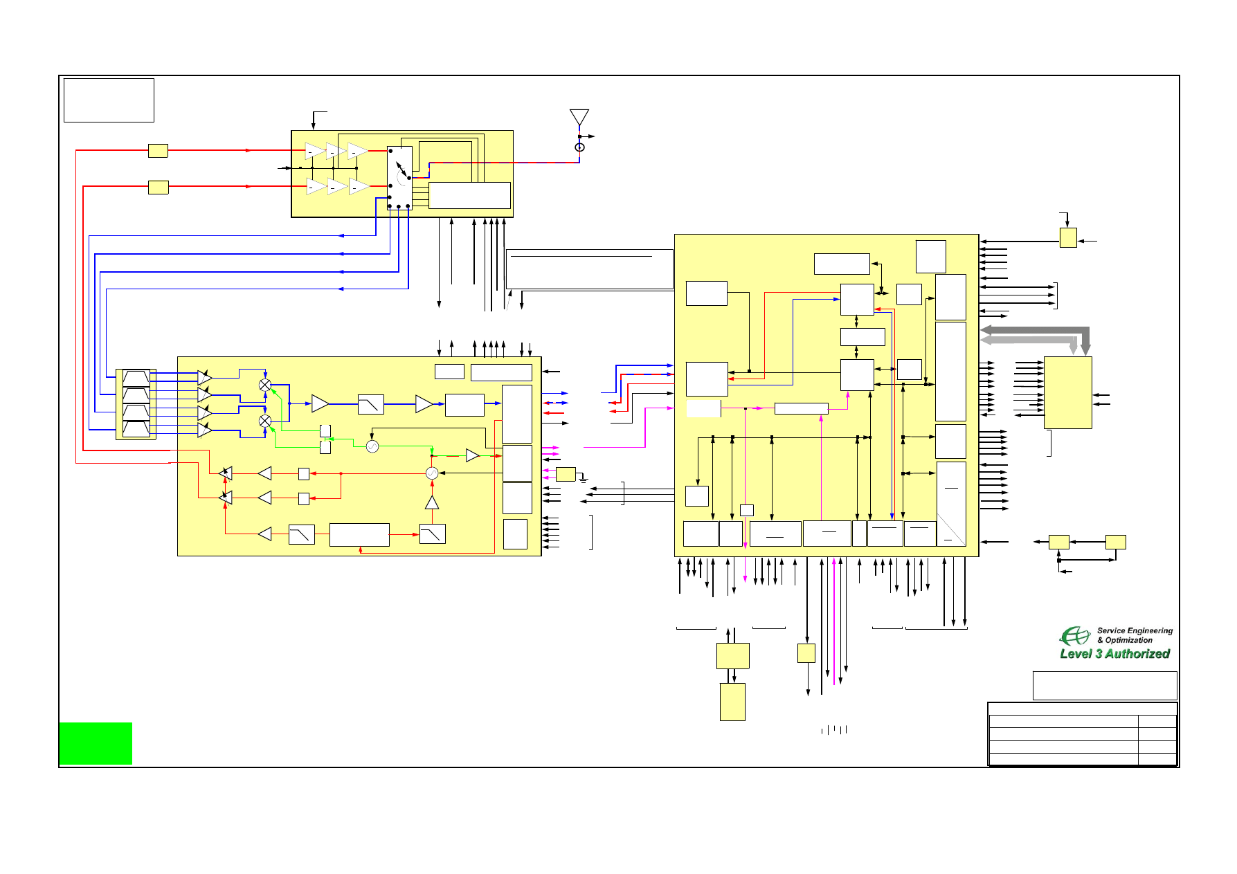
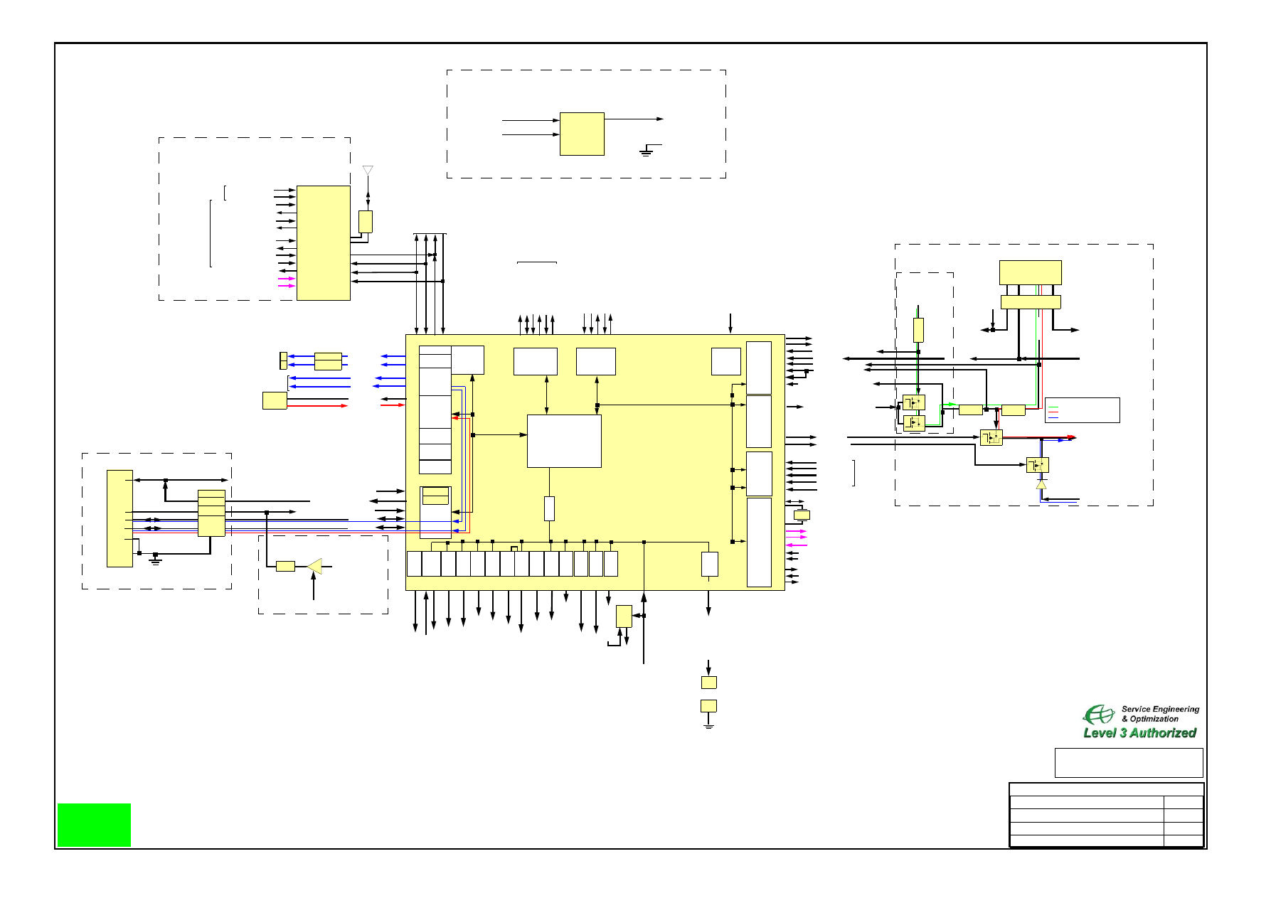
Z3
3
3
2
2
1
1
LNA
LNA
LNA
TX_HB
DCS/PCS OUT
GSM850/
BP
15
11,14....
26
25
GSM900 OUT
Se
ria
l
Inte
rface
D1
E3
G3
1
PA + Antenna Switch
6
13 8
E1
D2
F1
MISOB
MS
MDI
DRI
VRA
M
P
Y100
26MHz
2
1
1800 MHz
1900 MHZ
850 MHz
900 MHz
(P
A Po
we
r Contr
o
l)
J7506 Mechanical
Antenna Switch
Internal
Antenna
M1
RES
E
T
B
US_
E
U
R
O
TX_
A
N
T
_S
W_
EN
TX_
S
T
A
R
T
F3
(T
ra
ns
m
itt E
n
able)
RF_CLK
RF_DATA
RF_CS
B3
PA Control
B9
C2 A2
E2
GPIO
(U250 Control Bus)
ADC
Voltage
Reg.
VM_REG
VBUCK
RF_REG
J5, J8
H2
B4
(VCC’s from Atlas)
A4
1Mbit RAM
DSP
DSP
UltraLite
104 MHz
DSP Peripherals
accelerator, encryption
Timer, Interupts
Shared Memory
MCU
52 MHz
ARM7
MCU
26 MHz
Oscillator
Memory
Memory
SIM
Interface
External
Interface
Memory
N10
Clock Generator
SPI
Power
NEPTUNE LTE2
U800
W10
U9
T8
GPIO
L1 Timer
U6
U8
V7
W9
UART / USB
Interface
Keypad
Interface
On
Off
SIM DIO
SIM RST
SIM CLK
SIM_PD
VSIM_EN
VBUCK
(VCC + 1,875V)
(from Atlas )
VSIM
(to Atlas)
IO_REG
J4
L1
K3
R1
M1
K2
(from Atlas )
PERIPH_IO_REG
EGSM: CH 37 -- 942,4Mhz
DCS: CH 700 -- 1842,8MHz
PCS: CH 661 -- 1960MHz
RX MID CHANNELS
GSM: CH 62 -- 947,4 MHz
850: CH190 -- 881,6
MQSPI
Display
U700
EB1B
EB0B
OEB
R_WB
CS1BA
ADDRESS BUS
DATA BUS
K16
J19
G17
T16
BURSTCLK
LBAB
CS0BA
ECBB
V17
T19
L16
N18
A0-23
D0-15
64 MB Flash
RESET OUT
F3
C2
G8
E5
F5,D5
J2,H1,H8
G7
C6
K1
F4
D6
HS INT
C14
TF_ENABLE
16 MB SRam
(from Neptune)
FLASH
U13
BB
_SA
P
_T
X
B
B
_
S
AP
_R
X
BB
_SA
P
_
F
S
BB
_S
A
P
_
C
LK
B13
B12
A12
D13
(fram
es
y
n
c)
(cl
o
ck)
CLK
13 MH
z
W13
C15
C16
D15
A16
BB
_
S
P
I_C
LK
BB
_S
PI_M
O
S
I
B
B
_S
PI_
M
IS
O
AU
L_
CS
Neptune Atlas
Communication
T11
V12
V11
W12
ST
AN
DB
Y_1
_5V
G8
ST
A
N
DB
Y
CL
K 32
KH
Z
E3
B14
AU
L_
INT
RE
SET
B
V13
(13 M
H
z)
(W
a
tchdog)
WD
OG
OW
B
W11
On
e W
ire dat
a from
B
at
te
ry
US
B_V
P
IN
U
S
B
_
XR
XD
_
R
T
S
US
B_V
P
O
U
T
_
TX
D
US
B_V
M
IN_R
XD
U
S
B
_
TX
EN
B
US
B_S
E
0
B16
A17
Neptune Atlas
USB/ RS232
Communication
(t
o At
las
)
RE
SET
O
U
T
W5
(t
o U700)
(from/ to Neptune
Serial Audio for Ringtone
and Voice Audio)
BL
UE
_R
X
B
L
U
E
_T
X
B
L
U
E
_R
TS
B
B
L
U
E
_C
TS
B
N17
N13
V16
D16
(from/ to U301 BT, J1300
Neptune - BT - Neptune
Communication and Wakeup)
BLU
E_
W
A
KE
B
B
L
UE
_H
OS
T_W
A
K
E
B
D19
B15
KB
R0
-7
KB
C
0
-2
F3....
F2....
Timer
GPIO
Interface
BaseBand
Port Interface
Serial Audio
(tx)
(rx)
MQSPI
One
Bus
Wire
UART2
Universal
Asynchron.
Rx /Tx
BT
CS2B
W18
W8
T10
GA
_
INT
9
LB_
HB
C3
TX
_E
N
2
3
4
Power and
Antenna
Control
16
A1
3
K4
K5
LNA
TX_LB
L8
L10
2
4
(fro
m A
tl
as
)
VBUCK
E4...
(from
Atlas
)
U801
Level
(t
o Atlas
)
P2
LCD_RS
N3
LCD_CS
L3...
ATI_DQ (0 - 7)
(LCD Control to U5000 )
U1401
4
5
Hall Effect
Inverter
Shift
(VCC + 1,575V)
REF_REG
E2
A
TI_
RES
E
T
B
_2
_7V
U11
(t
o
U
5
000
)
(VCC + 2.775V)
A11, U16, .....
(VCC + 2.775V)
H1
V5, R16, ....
TOUT12
U10
(Bias output for THERM signal)
(Clock )
(Reset )
(Data In /OUT)
(T
rans
mit
t E
n
abl
e
)
(Clock )
(Chip select)
(Data In /OUT)
10
(fro
m A
tl
as
)
T18
(Trans Flash Enable to J4, Q2000 )
ANT_DET_B
(indicates mechanical Antenna connection to U800)
ANT_DET_B
U12
(indicates mechanical Antenna connection to U800)
EL_NAV_EN
N9
(EL Backlight Enable to U1501)
17
IPC
_
BC
M
B2
VCO_REG
18,31
RA61
RA60
2
2
4
4
FL100
Quard Saw Filter
4
3
Low Band
850MHz
Low Band
900MHz
High Band
1800MHz
High Band
1900MHz
6
1
and Matching
14
15
12
13
8
9
10
11
K12
L12
G12
H12
A12
B12
D12
E12
DC
Correct
LPF
÷
4
90°
÷
2
90°
÷
2
÷
2
LPF
LPF
Transmit
Modulator
TX CP
RX CP
Phase Modulation
Amplitude Modulation
TX VCO
RX VCO
VCO_REG
C10
IO_REG
C1
Digital Radio
Receiver
Synt
hesize
r
RX /
TX
Cl
ock
RX /
TX
In
/ O
u
t -
P
u
t c
o
n
tr
o
le
r
MCLK
G2
(Data TX)
(TX/RX Enable)
(Data RX)
(readback)
J1
BT_CLK
J3
BT_CLK_EN
G1
STANDBYB
VD
ET
EC
T
A4
REF_1p2
C5
D18
LCD_WEB
B
T
_
R
ES
ET
_B
T7
(from / to JDaughter Board Connector
EMU_HDST_DET
A12
(to Atlas U900 )
5,6
3
2
IO_REG
BP
REG_BYP_CORE
Switch
M18
(Flip Open/ Close
Detect)
1
6
PERIPH_IO_REG
U1600
2
Servive, Engineering & Optimization
2006.11.02
LEVEL 3 AL Block Diagram
Rev. 1.1
Z3
Page 1of 2
Key-Matrix
0-9,*,#
Navigation,
Smart,
Volume
(from
J
U50
0
0
)
D14
LCD_OEB
TRANSAM
U250 -
Revision Overview
Rev. 1.0: Initial Block Diagram
updated EL Circuit to U3000
(only used in Engineering debug mode
1. IPC: Input Power Control mode - for EDGE mode
2.BCM: Bias Control mode - for GMSK mode
(PA gain is fixed and PA input power varies)
(PA gain varies according to power step and fixed input PA power)
PA Power Control selection via VRAMP, TX_HB and TX_LB
- not for Service)
GSM / EDGE Tranceiver IC
RAPTOR
U50 -
Camera
FL1501
FL1502
EMI & ESD
NEP_CAM_TOURCH_EN
T6
(to Atlas U900)
U807
(Enable)
AD_TRIG
A12
(to Atlas U900)
Z3
(clock)
CLK 13 MHZ
V12
CLK_32KHZ_2_7V
P16
TIMER
WDOG
K10
CNTL.
PRI SPI
LOGIC
Logic
V
3
, J
4
...
...
..
Switcher
B
B
-S
PI_
C
LK
B
B
_
S
P
I_M
OS
I
B
B
_S
PI_
M
IS
O
AU
L CS
U1
8
U1
6
T18
T1
7
R5
Interface
USB
Y900
V17
D12
RTC_BATT
V16
BP
SPKRM
SPKRP
T6
R7
T9
P9
V10
U8
PW
R_
SW
F1
4
B4
E3
F3
U900
ATLAS UL
ON
LOGIC
OWB
THERM
P13
THERM
BATTP
D14
GND
CHRGCTRL
B16
VBUS
S
G
D
CHARGE
Charger
BATT CONN.
CNTL.
LED
E12
BB_
SA
P_F
S
BB
_SA
P
_C
LK
B
B
_S
AP
_TX
B
B
_S
AP
_RX
CODEC
16 BIT
STEREO
(tx) (rx)
ALERTM
ALERTP
STANDBY
F12
(to Neptune and U301 BT)
AUL
_IN
T
N14
RESETB
(from U800)
Neptune Atlas
Communication
USB_ID
H8
Q904 (M3)
G
S
BP
B12
BATTFET
Battery to BPLUS
U
S
B_
VP
IN
U
S
B_
XR
XD_
R
TS
US
B
_
V
P
O
U
T_
TX
D
U
S
B_
VM
IN_
R
X
D
U
S
B_
TX
ENB
US
B
_
S
E
0
USB/RS232
(communication)
B2
C4
F4
B1
B3
E4
MICINM
MICBIAS1
Det.
Stereo
B
o
os
t 3
00mA
G1
6
Switcher
B
u
ck 350mA
F1
6
( 1,
8
75V
)
VB
UC
K
H2
( 2,
77
5V
)
PER
IPH
_I
O_ RE
G
U6
M1
8
K1
7
H4
H3
( 2,
77
5V
)
RF
_R
E
G
L1
6
( 1
,575
V
)
R
E
F
_RE
G
N5
( 1,
8/
3
V
)
VS
IM
VS
IM
_EN
K1
1
VBUS
CONTR.
AD
C15
PE
RI
P
H
RE
G
(B
ia
s)
(One Wire Bus
to Neptune)
BPFET_PM
VBUS to BP
Switch
(Main Source
for Atlas)
(from Mini USB Connector)
Main Charge Path
B+ support without Ext Charger
B+ support with Ext Charger
Color definition only for this section !
D903
BB_SAP_TX
BB_SAP_RX
BB_SAP_FS
BB_SAP_CLK
(framesync)
Bluetooth
U301
C7
BLUE_WAKEB
C8
BLUE_HOST_WAKEB
C6
BLUE_RX
E5
BLUE_CTSB
BLUE_RTSB
E7
BLUE_TX
E4
E8
BT_RESET_B
E3
(from/ to Neptune
Serial Audio for Ringtone
and Voice Audio)
PERIPH_IO_REG
B3......
BP
H6
BT
_A
NT
25
Strip Line
Antenna
(on PCB)
F6
VV
IB
(from Neptune)
NeptuneAtlas
Neptune Atlas
USB/ RS232
Communication
(Battery Sense)
(VBUS Sense)
CONV.
D/A
CLK_32KHZ
(from Atlas)
3
(from Atlas)
( 1,
3V
)
(from/ to U301 BT,
Neptune - BT - Neptune
Communication and Wakeup)
Internal MIC
PCB
Pads
ADTRIG
(TX_START)
U15
(from Neptune, Tx Mode indication for Atlas)
( 2,
77
5
)
IO
_RE
G
( 2,
77
5 )
CAM
_
A
V
D
D
( 5,
5V
)
VB
OO
ST
2
3
VBUS
1
4
5
(to Charging Circuit)
G1-G4
(Shield)
CLK_32KHZ
R16
DM_TXD
DP_RXD
VBUS 5V
Pass FET
VBOOST
VBUS
D2
(PPD device support)
(from J1300)
(to U5000)
to
V
ib
ra
tor
VIB REG
P2
Mo
to
r
RE
F R
E
G
RF REG
PE
R
IP
H
IO REG
AUDIO
REG
IO
REG
GR
A
P
H
REG
CA
M
E
RA
REG
P1
8
DIG
REG
4
Microphone
R3
P4
R4
(t
x)
(r
x)
13 Bit
Handset
Amplifier
(to J2)
Q9
10
VC
O
RE
G
VC
O
_
D
R
V
(M
ain
Sour
c
e-
f
rom Q904)
( 2,
77
5V
)
VC
O_R
E
G
V2
SIM_PD
T14
CHRGRAW
S
G
D
Q903 (M4)
Q905
G
S
R910
R911
D
Switch
B14
CHRGISNSP
E15
(Current Control)
Q906
C6
BLED_SINK1
(t
o Neptu
n
e)
(t
o
J
200
0, Q2020)
(t
o Nept
une amd
(t
o U2
50)
(t
o AL
+
R
F
))
(t
o
U50,U250)
Bluetooth
Mini USB
Charger and Power-
source Control
(to Neptune, U250)
(toNeptune)
(from Atlas)
(from Neptune)
TOUT12
(Bias Voltage from
Neptune)
(Accessory Detection signal)
(from Acesory Connector)
(EXT Power)
(EXT Power)
Det.
Headset
(from J600)
R90
5
3
4
1
ESD
VR960
VR1203
VR970
SAP
Supply
Amplifier
Alert
Amplifier
Headset
Amplifier
EMU
J1
NC
NC
ALERT
NC
ESD
FL1400
2
2
BA
TT
P
J3
2
3
1
4
VR1201
B
+
Sens
e
(t
o J
J600,
U3000
ISNS
F13
(Batt Current)
(Charger Current + )
NC
M1401
1
2
U14
CHRGLED
L10
(toJ600)
STANDBYB
P14
(to U250)
B6
BLED_SINK2
D6
BLED_SINK3
F8
BLED_SINK4
K1
6
(2
,7
75
V
)
VM
_
R
E
G
(t
o U2
50)
VS
IM
RF REG
(f
ro
m U
800)
(t
o
AL + RF
))
(t
o AL
+
R
F
))
VIB Motor
R1
7
REF REG
( 1,
2V
)
RE
F_
1P2
(t
o U2
50)
U950
R950
PERIPH_IO_ REG
EMU_HDST_DET
(Headset detect Enable from Neptune)
(Bias from Atlas)
(100K Headset
STANDBY
C4
BT_CLK_EN
D7
(to U250)
A7
B6
C7
FL
30
1
H1
H2
E2
BT_CLK
(from U250)
detect Resistor)
Headset detect circuit
Servive, Engineering & Optimization
2006.11.02
LEVEL 3 AL Block Diagram
Rev. 1.1
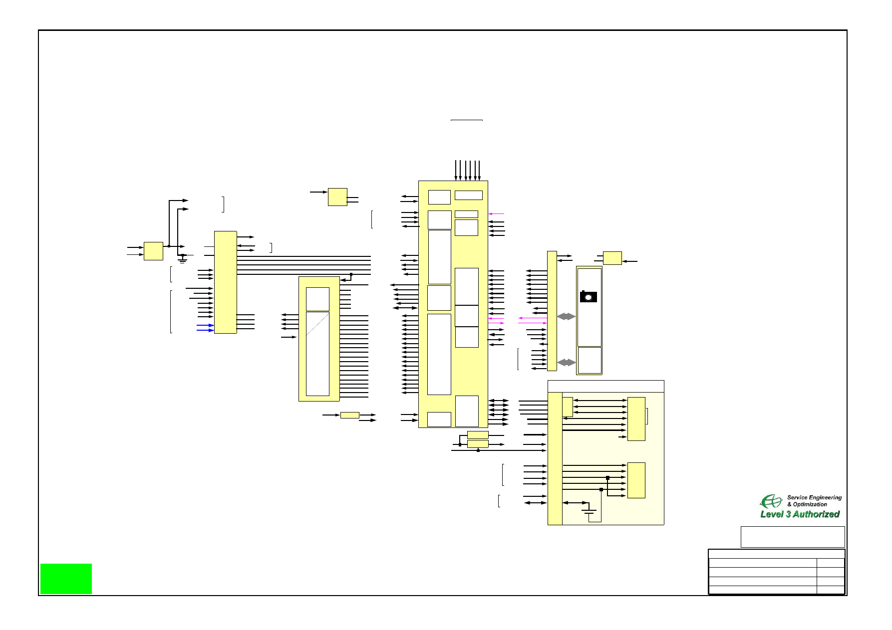
Z3
Page 2of 2
1
E10
LED_BT
(from J600)
NC
NC
Daughter
B
o
ar
d)
EL_NAV_EN
EL_LAMP_VP
EL_LAMP_VM
VBOOST
8
3
10
U3000
EL Driver
EL Backlight Driver
(enable from Neptune)
Revision Overview
Rev. 1.0: Initial Block Diagram
updated EL Circuit to U3000
Z3
Servive, Engineering & Optimization
2006.10.10
LEVEL 3 AL Block Diagram
Rev. 1.0
Z3
Page 2of 2
Revision Overview
Rev. 1.0: Initial Block Diagram
U8096
G6
F5
G5
E4
G4
F4
D4
D6
D5
E6
E5
F6
C6
C5
B6
B5
A6
LCDC_RED5
LCDC_RED4
LCDC_RED3
LCDC_RED2
LCDC_RED1
LCDC_RED0
LCDC_GREEN5
LCDC_GREEN4
LCDC_GREEN3
LCDC_GREEN2
LCDC_GREEN1
LCDC_GREEN0
LCDC_BLUE0
LCDC_BLUE2
LCDC_BLUE3
LCDC_BLUE4
LCDC_BLUE1
Serializer
A5
C1,D2
LCDC_BLUE5
GND
J5
N2
H4
K4
M2
J5
M5
M1
L5
K5
L1
L4
M4
N1
N5
P2
N4
P4
G2
LCDC_OE
LCDC_GS
LCDC_LS
LCDC_CLK
(Neptume / ATI
Communication Bus
B
N1
9
P1
5
BB_SAP_CLK
BB_SAP_FS
BB_SAP_TX
BB_SAP_RX
(ATI- Neptune
Communication)
Camera /Display
Graphics Accelerator
ATI
U5000
Tri-Flash -Neptune
V1
V2
V4
W2
LCDC_SD
R2
T1
R1
P1
F1
D19
D15
C19
B19
D14
E19
J2000
CAMERA
CONNECTOR
22
1
2
5
7
9
10
15
11
12
13
14
6
16
3
23
CAM_PWRDWN
CAM_SCL
CLK0
D_CAM(0)
D_CAM(1)
D_CAM(2)
D_CAM(3)
HS
CAM_RESET
VS
CLKI
D_CAM(7)
D_CAM(6)
D_CAM(5)
D_CAM(4)
H1
W6
R6
T6
T7
V6
W8
L2
V8
W9
R9
R8
T8
R7
E1
4
VBUCK
IO_REG
U19
CLK_32KHZ_2_7V
RGB Data
Image Data
Sync.
W7
CAM_SDA
V7
Control
(H Sync)
(VSync)
Output Enable
Data Clock
Serial Data
GPIO (ID)
SDIO
Interface
Control
Serial
Power
Timer
SPI
Tri Flash Write Data)
GA
_IN
T
PERIPH_IO_REG
(GRAPH_REG)
(Horizontal Sync)
(Vertical Sync)
KBR0
KBR3
KBR4
KBR6
CBC2
(from/ to
Neptune)
28
26
27
30
29
CAM_AVDD
19
BUCK_SW
20
2MP
Camera
Keys:
Volume
Smart
Voice Cmd
LCDC_PID1
SER_CLKP
SER_CLKM
SER_DATAP
SER_DATAM
D1
E1
G1
F1
32
30
24
26
J600
Slider Connector
SPKRP
SPKRM
27
29
BLED_SINK4
BLED_SINK3
BLED_SINK2
BLED_SINK1
7
9
11
13
C3
C4
B4
A3
B3
LC
D_
R
S
A
T
I_
DQ
(0 - 7)
LC
D_
WE
B
LC
D_
O
E
B
P1
9
GPIO
LCDC_SCLK
LCDC_SDI
LCDC_DO
LCDC_CSB
B3
G1
C1
B2
15
17
19
21
CHRGLED
33
VBUS
35
VBOOST
IO_REG
VBUCK
1
3
5
EL__NAV_EN
EL_COM
EL2
VBOOST
8
3
10
U3000
EL Driver
(VCC)
(Enable from Neptune)
4
6
LCDC_RESETB
36
D1
(VCC from Atlas)
(from Mini USB)
(from Atlas)
KPR0-5
KPC1-2
10.....
18...
PWR_SW
10.....
(to Atlas)
(from/ to Neptune)
G2
G3
SER_EN
F2
LED_BT
23
VBUCK
FLASH_TORCH_EN
FLASH_DRIVER_EN
J2
K2
J400
Pogo Pins for
1
3
Camera Flash Connector
4
2
B+
GND
(VCC from Atlas)
(VCC from Atlas)
4
5
2,3
VBUCK
Switch
Q2020
Parallel
Serial
Control
A2...
V19
H7
GRFX_REG
R19...
SD0
SD1
SD2
SD3
SD_CMD
SD_CLK
(from/ to Neptune)
LCDC_PID2
H2
R5002
PERIPH_IO_REG
GND
(LCD ID Resistor)
H1
6
A
T
I_
RE
SE
TB
_2_
7V
Interface
H1
9.
.
GPIO
J4
1
3
5
9
11
13
D
aughter
Boar
d Connec
tor
FL120
0
14
T
ransflash
7
8
1
2
3
5
4
TF_VDD
TF_ENABLE
12
G1-G3
GND
SIM
1
2
3
4
5
6
SIM_DIO
SIM_CLK
VSIM
SIM_RST
GND
8
2
6
4
15..
10
+
RTC_BATT
RTC
BATT
Daughter Board
TF_DET
TF_VDD
7
PERIPH_IO_REG
Q2000
R1209
(from/ to Atlas)
TP712_EL_COM
TP_EL2
EL Main PCB Contact
Wyszukiwarka
Podobne podstrony:
BD V600 L3 C A3 V1[1] 1
BD C150 L3 C A3 V1[1] 2
BD TripletsR L3 C A3 V1[1] 1
BD V3 L3 C A3 V1[1] 2
BD C200 L3 C A3 v1[1] 0
BD U9 L3 C A3 V1 0
BD F3 L3 C A3 v1
BD K1 L3 C A3 V1 3
BD BlDi V235 L3 C A3 V1[1] 1
Block Diagram W510 L3 C A3 V1 0 Block Diagrams
Block Diagram V3 06 L3 C A3 v1 0
BD W206 W213 A3 C L3 V1
C380 PCB P4c L3 A3 BW V1 0
BL C380 P4c L3 A3 BW V1[1] 0
BL C650 P03 L3 A3 BW V1(1)
BD BlDi E365 A3 C L3 1[1] 2 030611100711
excel bd z3 spr2b
więcej podobnych podstron